Ass. Prof. Sakellaris Mailis
The available projects are designed to introduce students to standard cleanroom-based fabrication/processing methods (photolithography, materials deposition, surface analysis), optical spectroscopy (Raman, PL), various advanced imaging techniques (scanning electron microscopy, atomic force microscopy, focussed ion beam, transmission electron microscopy) as well as other optical and electronic material/device characterization techniques.
If you are interested in completing one of the MSc projects presented below – please contact Prof. Sakellaris Mailis ().
Background:
Ultrathin, single or few layer materials have attracted much attention after the isolation of graphene. Since then, a plethora of ultrathin single atomic/molecular materials have been identified that provide of tailoring of materials to match various applications in electronics and photonics. We have developed a laser synthesis method that enables the manufacturing of 2D transition metal disulphides at ambient conditions, which i) simplifies the, normally complex, growth methodology and ii) produces ready patterned films.
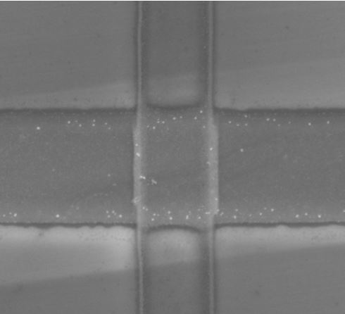
 A laser -printed MoS2/WS2 heterostructure.
Currently, we are exploring this direct laser-printing method by:
– Conducting an in-depth investigation of the physical properties of these materials using spectroscopic and other analytical methods to identify their suitability for various sensing applications, including optical and chemical sensors.
– Expanding the range of 2D materials that can be grown using this method. After demonstrating the laser printing of MoS2 WS2 and their alloys, we are now exploring other 2D transition metal dichalcogenides, of the selenide family, which possess complementary electronic and photonic properties to transition metal disulphides.
– Producing new hybrid materials by combining TMDs with carbon nanomaterials (single wall carbon nanotubes and graphene) and other porous semiconductors.
Learning Outcome:
By the end of the project the student will be able to:
- Knowledge: discuss the Physics of 2D semiconductor materials, identify suitable material growth methods as a function of applications, discuss the dynamics of thermal dissociation of chemical precursors, discuss the Physics of Gaussian beam propagation, focussing and laser imaging.
- Skills: Employ data acquisition methods, extract and analyse experimental data, perform basic cleanroom processes, build and optimize complex optical and electrical experimental arrangements, present research results.
- Experience: Employ standard cleanroom processes, use advanced spectroscopic and imaging tools, compose and present scientific reports.
Highlighted Publications:
[1] “Laser printed two-dimensional transition metal dichalcogenides”, O. Abbas et al., Sci. Rep. 11 (5211) (2021)
Background:
Due to the versatility and technological applicability of direct laser writing method, localised hybridization/heterostructuring of carbon nanomaterials and noncarbon layered nanomaterials, mainly transition metal dichalcogenides and oxides, can be established. This project focuses on:
– Localised conformal deposition of TMDC on carbon nanotube templates.
– Laser heterostructuring of 2D transition metal dichalcogenides and 2D metal monochalcogenides, e.g. SnS.
– Study the structural, optical and electrical characteristics of these composites.
Learning Outcome:
By the end of the project the student will be able to:
- Knowledge: discuss the Physics of 2D semiconductor and carbon based nanomaterials, identify suitable material growth methods as a function of applications, discuss the dynamics of thermal dissociation of chemical precursors, discuss the Physics of Gaussian beam propagation, focussing and laser imaging,
- Skills: Employ data acquisition methods, extract and analyse experimental data, perform basic cleanroom processes, build and optimize complex optical and electrical experimental arrangements, present research results.
- Experience: Use standard cleanroom processes, use advanced spectroscopic and imaging tools, compose and present scientific reports.
Background:
Spatially selective laser irradiation is employed to modify the photonic and electrical properties of photonic and electronic materials. We are exploring the strong interaction of laser radiation with various materials such as semiconductors and other crystalline and amorphous materials to modify locally the refractive index, charge transport and the surface topography to achieve tailoring of device performance and to produce optical waveguide circuits as well as diffractive optical elements.

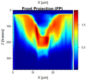
Localised laser-induced densification of porous Si.
We are currently exploring porous silicon and thin film Lithium Niobate as potential photonic platforms.
Learning Outcome:
By the end of the project the student will be able to:
- Knowledge: discuss the Physics of laser-mater interaction, discuss the Physics of optical waveguide propagation, discuss the Physics of Gaussian beam propagation, focussing and laser imaging, Discuss the Physics of optical ferroelectric materials.
- Skills: Employ data acquisition methods, extract and analyse experimental data, perform basic cleanroom processes, build and optimize complex optical and electrical experimental arrangements, present research results.
- Experience: Use standard cleanroom processes, use advanced spectroscopic and imaging tools, compose and present scientific reports.
Highlighted Publications:
[1] “UV laser-induced nanostructured porous oxide in GaAs crystals”, I. Salimon et al., Solid State Sciences 128, 106887 (2022)