Abstract: The semiconductor nanowires (NWs), which are crystalline structures with diameters from tens to hundreds nanometers and lengths up to 100 micrometers, attracts increasing attention. To date, they have been synthesized based on virtually all known semiconductor compounds already. NWs can be used as a basis for the creation of different opto- and nanoelectronics devices with higher functionality, and at the same time, these devices are being developed on both single and nanowire arrays. Therefore, the synthesis of uniform arrays of NWs are of importance for many applications. The questions concerning the molecular-beam epitaxial synthesis of such nanowire arrays based on the use of colloidal gold nanoparticles will be considered at this seminar. Furthemore, it should be noted, that there are many difficulties, which limit the massive use of devices created on their basis. Among them, it is worth highlighting the problems associated with the creation of electrical contacts to single NWs. One of the possible solution of this problem, which we are proposed, is the use of cost effective method – the dielectrophoretic (DEP) assembly.
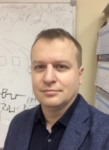
Biography: Alexei D. Bouravleuv received the Graduation degrees in physics from the St. Petersburg State Polytechnikal University, St. Petersburg, Russia, the Ph.D. and Dr.Sc. degrees in physics and mathematics from Ioffe Physical Technical Institute RAS and Institute for Analytical Instrumentations RAS, in St. Petersburg, in 2002 and 2014, respectively. After posdoctorals years in Tokyo University of Agriculture and Technology, Tokyo, Japan, he joined Ioffe Institute RAS, St.Petersburg, Russia as a senior researcher and, later on, St.Petersburg Academic University RAS. To date, he is the head of Nanoelectronics laboratory of St.Petersburg Academic University RAS, St. Petersburg, Russia. His research interests include the study of epitaxial growth and properties of various semiconductor nanostructures based on different materials, such as A3B5 compounds, Si, Ge, dilute magnetic semiconductors, as well as wide band gap materials, which can be used for the creation of novel opto-, nanoelectronics and spintronics devices.
